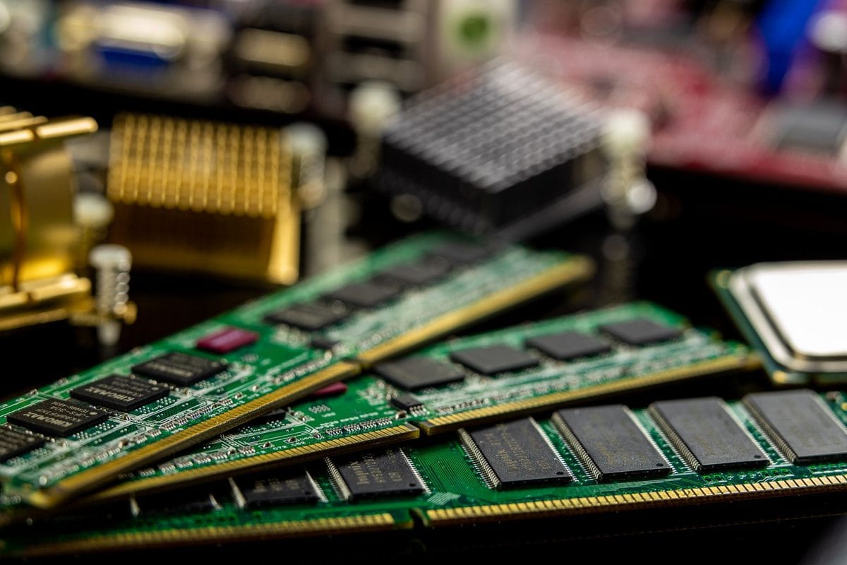
Korea's SK Hynix, Samsung Electronics and US-based Micron are racing to bring HBM4 memory into mass production, the next generation of high-bandwidth memory chips that sit at the center of every major AI accelerator on the market. The shift marks a structural change for an industry that used to treat memory as a commodity business defined by price cycles, not by who can pack the most bandwidth next to a processor die.
HBM, short for high-bandwidth memory, stacks multiple layers of DRAM vertically and connects them to a processor through thousands of short interconnects, delivering far more data throughput per watt than conventional memory modules. Nvidia's data-center GPUs, along with AMD's competing accelerators, depend on HBM to keep pace with the computational demands of large AI models, and each new GPU generation has required a corresponding jump in memory bandwidth and capacity.
SK Hynix Holds the Lead Position
SK Hynix has positioned itself as the primary HBM supplier to Nvidia through recent GPU generations, having been first among the major memory makers to pass Nvidia's qualification process for HBM3E, the current-generation standard that HBM4 will succeed. That early qualification translated into a dominant share of a market segment that barely existed five years ago and now accounts for a growing portion of the company's overall memory revenue.
Moving to HBM4 raises the technical bar considerably. The new standard widens the interface between memory and processor, increasing the number of data channels while pushing per-stack bandwidth well beyond what HBM3E delivers. SK Hynix has said it intends to begin mass production of HBM4 within 2026, aligning its timeline with Nvidia's next major GPU architecture, which is expected to require the new memory standard to hit its performance targets.
Samsung's Catch-Up Effort
Samsung, the world's largest memory chipmaker by revenue, has struggled to match SK Hynix's pace in HBM qualification over the past two years. The company has repeatedly said it is working through Nvidia's certification process for its HBM3E products while simultaneously developing HBM4, effectively fighting on two fronts at once. Samsung's advantage lies elsewhere: it controls both memory fabrication and advanced packaging under one roof, along with a foundry business that can manufacture the base logic die that sits underneath an HBM stack — a capability neither SK Hynix nor Micron has in-house at the same scale.
Whether that vertical integration translates into a faster HBM4 ramp remains an open question. Packaging yield, not raw memory design, has been the more common bottleneck across the industry, since stacking eight or twelve DRAM layers with thousands of through-silicon vias demands near-perfect process control at every layer.
Micron's Quieter Push
Micron, based in the United States but reliant heavily on fabrication and assembly operations across Asia, including Taiwan and Singapore, has emerged as a credible third supplier rather than a distant follower. The company has shipped HBM3E in volume to data-center customers and has outlined its own HBM4 roadmap, betting that even a smaller share of a rapidly expanding market is worth more than a larger share of conventional DRAM sold at commodity margins.
That bet reflects a broader pattern across the industry: AI accelerator demand from hyperscale cloud operators has grown fast enough that even the number-two or number-three HBM supplier can sell everything it produces, at pricing well above standard DRAM.
The DRAM Squeeze Behind the Headlines
Producing HBM absorbs disproportionate wafer capacity relative to conventional DRAM, since each HBM stack requires several DRAM dies bonded together along with the manufacturing steps needed for through-silicon vias. As SK Hynix, Samsung and Micron redirect production lines toward HBM, they pull capacity away from the DRAM used in laptops, smartphones and servers — a dynamic that industry analysts have linked to tighter conventional memory supply and firmer pricing in 2025 and into 2026.
- Conventional server and PC DRAM has tightened as fabs convert lines to HBM production.
- Mobile DRAM suppliers have faced longer lead times as capacity gets reallocated.
- Some smaller memory makers in the region have shifted focus toward legacy and specialty DRAM segments the big three are vacating, a niche that is becoming more valuable simply because fewer suppliers still serve it.
What HBM4 Changes Technically
Beyond raw bandwidth, HBM4 introduces a wider 2,048-bit interface per stack, roughly double the width used in HBM3E, along with support for a customized base die that GPU makers can design to their own specifications rather than relying on a standard logic layer supplied by the memory maker. That customization option, if adopted, would let companies like Nvidia tune the base die's power delivery and signal routing specifically for their own accelerator architecture, tightening the relationship between memory suppliers and their largest customers even further.
JEDEC, the industry body that standardizes memory specifications, finalized the core HBM4 standard to give chipmakers a common target, though individual suppliers still differentiate on stack height, thermal performance and the custom base-die option described above.
Capacity Commitments and Regional Stakes
All three companies have announced expansions to their HBM and advanced packaging capacity in Korea, Taiwan and the United States, reflecting how central this segment has become to national industrial strategy as well as corporate revenue. Korea in particular has framed HBM leadership as a strategic asset, given that SK Hynix and Samsung together represent the overwhelming majority of global HBM output.
Taiwan's role sits mostly in packaging rather than memory fabrication itself, since TSMC provides advanced packaging services that some HBM stacks and their associated logic dies pass through before reaching GPU assembly lines — another link in a supply chain that now runs through multiple countries before a single AI server rack gets built.
What Comes Next
The near-term test for all three suppliers is qualification: passing the technical validation that Nvidia, AMD and other accelerator makers run before committing to large-volume orders. SK Hynix's head start on HBM3E does not guarantee it repeats that position with HBM4, since Samsung and Micron have had more time this cycle to prepare their own submissions in parallel with the standard's finalization.
For now, the companies are shipping what qualified capacity they have as fast as they can build it, with order books for 2026 and 2027 already shaping how much wafer capacity each supplier commits to HBM versus the conventional memory markets they are gradually deprioritizing.